
Highlight Photo
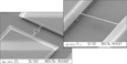
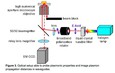
Collaborative project: Systematic near-field and far-field study of surface plasmon propagation in polycrystalline and single-crystal Ag waveguides at visible frequencies
STM image of Ag film on Si
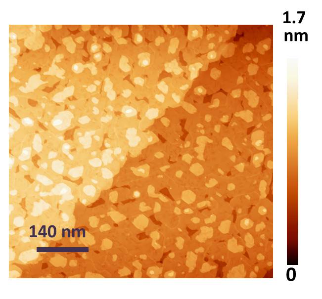
Fig. 1. STM image of Ag film on Si. The light patches are one-atom-high clusters of Ag atoms, while the darker patches are small pits the depth of one atomic layer. We can refer to this surface quality as “plus or minus one atomic layer,” which is excellent for Ag film. The diagonal boundary running from the bottom left to the top right of the image is an atomic step in the underlying Si substrate.
Credits: Jisun Kim