

Highlight
Collaborative project: Systematic near-field and far-field study of surface plasmon propagation in polycrystalline and single-crystal Ag waveguides at visible frequencies
STM image of Ag film on Si
Achievement/Results
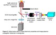
With computer processing requirements always increasing, signal transmission speed within electronic circuitry is becoming a limiting factor in the further increase of processor efficiency.1 It is therefore important to find new types of circuitry that can transmit signals more quickly than traditional electronic circuits. Additionally, such circuitry must be amenable to large-scale industrial device fabrication.
A team of five graduate student researchers from the University of Texas (UT) at Austin—Charlotte Sanders and Guru Khalsa (Physics), Christopher Mann (Engineering), and Micah Glaz and Sarah Stranahan (Chemistry)—working with the support of an NSF Integrative Graduate Education and Research Traineeship (IGERT) program, has initiated a cross-disciplinary study to develop and characterize a class of circuits that is based not on simple electron flow, as in a traditional circuit, but on the transmission of plasmonic waves. Plasmonic waves are oscillations of electrons that occur when the electrons in a metal (or other type of conductor) interact with incident light to form travelling waves.
Towards the goal of plasmonic circuitry, we have completed two crucial steps: development of a technique to create robust high quality thin films of silver, far exceeding the quality of films in previous studies; and the ability to extend this technique to the fabrication of nano-circuitry. Plasmonic wires, known as “waveguides,” herd plasmonic waves in the same way that conventional wires guide electron flow in traditional electronics. Networks of waveguides can be assembled into plasmonic circuits to carry information from one point to another. Recent studies suggest that the signal speed enhancement can be as great as 100 times in some materials.2 In addition, if plasmonic structures could be fabricated on silicon (Si) wafers, then plasmonic circuits and traditional electronic circuits could be combined on a single chip.3 In order to make plasmonic circuitry possible, the following are required:
-
the ability to fabricate metal structures, preferably on Si, that can support the propagation of plasmonic waves over distances on the length scale of the circuit; and
-
the ability to fabricate waveguides out of these metal structures.
Neither of these is trivial. Most metals are not favorable to plasmonic waves, quickly absorbing the waves’ energy and converting it to heat. Furthermore, maximizing plasmonic wave propagation length requires that the metal structures in which the plasmons travel be of extremely high crystalline quality and very smooth. The ideal metal for plasmonics is silver (Ag), but with Ag, in particular, it has until now been difficult to achieve the strict requirements for crystalline quality and smoothness. Furthermore, the waveguides require precise control of very small dimensions, down to the nanometer, an issue that the semiconductor industry continues to struggle with, and innovate from. An investigation of this problem requires a wide range of expertise, ranging from nanoscale fabrication to optical characterization and theoretical interpretation. The IGERT program, by creating an environment that fosters interdisciplinary work and encouraging student research initiative, brought together five students from three departments at the University of Texas at Austin to conduct this study.
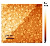
With financial support from IGERT, Charlotte Sanders, under the guidance of her doctoral advisor Dr. Chih-Kang Shih and in collaboration with research groups in both Austin and Beijing, has found a way to fabricate Ag structures on Si with the requisite crystallinity and smoothness. Using a home-built experimental setup constructed primarily in the University of Texas’s own machine shop, the Shih group developed a method for growing flat two-dimensional Ag films on Si with unprecedented smoothness, and have the ability to control the films’ thickness with atomic layer precision. The method is a form of molecular beam epitaxy (MBE), and can be easily adapted to large-scale industrial use, where MBE is already a workhorse. Sanders and her colleagues studied the film quality using the atomic-scale imaging capabilities of scanning tunnelling microscopy (STM); see Fig. 1. Their films were then sent to a collaborating group at the Chinese Academy Sciences, which carried out optical studies confirming that plasmons could propagate further than in similar films grown using previously existing methods. Sanders travelled to Dallas, TX this spring, with funds provided by her IGERT travel stipend, to report these findings at the American Physical Society’s March Meeting.
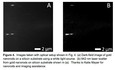
With this cornerstone laid, it became possible to move to the next phase of the project. The starting point was the design and construction by Mann of new technology for the fabrication of the high quality crystalline waveguides. Using techniques that are well established, or easily adapted to the semiconductor industry, various structures have been fabricated, such as those in Fig. 2, proving the viability of the technology. The group’s efforts in this area are ongoing; once the structures are reliably reproducible, they can be examined by optical techniques.
Sarah Stranahan, working under her doctoral advisor Professor Katherine Willets, has identified and tested an optical set-up, shown in Fig. 3, capable of interrogating the Ag waveguides. In order to demonstrate the compatibility of the optical system with the waveguides that are still under development, a gold nanoparticle system of similar size scale and on the same type of Si substrate was imaged, shown in Fig. 4.
This collaboration made possible by the NSF IGERT program has led to promising groundwork to improve the new technology of plasmonic circuits.
1 Mauro J. Kobrinsky et al., Intel Technology Journal 8, 129 (2004).
2 Vasily Temnov, et al., Optics Letters 32, 1235 (2007).
3 Ekmel Ozbay, Science 311, 193 (2006).
Address Goals
With computer processing requirements always increasing, signal transmission speed within electronic circuitry is becoming a limiting factor in the further increase of processor efficiency.1 It is important to find new types of circuitry that can transmit signals more quickly than traditional electronic circuits, and at the present time there are no viable options. This area of research is technologically important, and offers an opportunity for the U.S. to further strengthen its position as a global leader in science and engineering. Solutions that can be implemented at large scale and for low or moderate cost will promote American industry and economic growth in the 21st century. Furthermore, advanced computational capabilities are crucial to cutting-edge fundamental research in all fields.
Five graduate students supported by the University of Texas (UT) at Austin’s NSF Integrative Graduate Education and Research Traineeship (IGERT)—Charlotte Sanders and Guru Khalsa (Physics), Christopher Mann (Engineering), and Micah Glaz and Sarah Stranahan (Chemistry)—have initiated a cross-disciplinary study to develop and characterize a class of circuits that is based not on simple electron flow, as in a traditional circuit, but on the transmission of plasmonic waves. Plasmonic waves are oscillations of electrons that occur when the electrons in a metal (or other type of conductor) interact with incident light to form travelling waves. Plasmonic wires, known as “waveguides,” channel plasmonic waves in the same way that conventional wires guide electron flow in traditional electronics. Networks of waveguides can be assembled into plasmonic circuits to carry information from one point to another. Recent studies suggest that the signal speed enhancement can be as great as 100 times in some materials.2 In addition, if plasmonic structures could be fabricated on silicon (Si) wafers, then plasmonic circuits and traditional electronic circuits could be combined on a single chip.3
The completion of this project will constitute a significant step toward the realization of technologically and commercially viable plasmonic nanocircuitry enabling significantly enhanced processor speeds.
Secondary Goal: The current project, created by the graduate student collaborators themselves, was inspired by a grant-writing competition sponsored by UT IGERT. Competing for an educational stipend of $1000, they were asked to write and submit a formal research proposal in conformance with standard NSF guidelines. This gave them experience with grant writing, and required them to work collaboratively under a deadline, while thinking carefully about research funding and the global influence of their work.
All of the members of the current collaboration are actively involved in the planning and execution of the UT Austin/NSF IGERT Summer Nanoscience Academy (SNA), a three day workshop where middle and high school students from around Texas come to the University of Texas at Austin to learn about nanoscience from IGERT trainees and faculty. Methods and results from this plasmonic waveguiding project will be incorporated into this year’s curriculum. The SNA connects pre-college students with graduate students and faculty conducting cutting-edge research. Through lectures, tours, demonstrations, and hands-on labs the SNA gives the students a taste of nanoscience research and exposes them to its technological applications. In this year’s session, students will be given a presentation on the motivation and status of the project and will be involved in a trainee lead discussion of the potential applications. In addition, students will see Stranahan’s optical setup, and will also see the clean room facilities where Mann pursues part of the sample fabrication process.
The benefits of the SNA are enhanced and extended through a workshop that is provided to the teachers whose students participate in the academy. The workshop provides curriculum materials and is also a forum for preparation of lesson plans dealing with nanoscience topics. This year’s teachers will receive materials relating to plasmonics and nanoscale fabrication methods that they can use in the classroom.
1 Mauro J. Kobrinsky et al., Intel Technology Journal 8, 129 (2004).
2 Vasily Temnov, et al., Optics Letters 32, 1235 (2007).
3 Ekmel Ozbay, Science 311, 193 (2006).