
Highlight
Nanocrystal-based solar cells and scanning optical microscopy
CIGS nanocrystal-based “inks” for use in low cost solar cells
Achievement/Results
Facilitated by the National Science Foundation’s (NSF) Integrative Graduate Education and Research Traineeship (IGERT) program in Atomic and Molecular Imaging of Interfaces and Defects at The University of Texas at Austin, Ph.D. students Brian Goodfellow working under Prof. Brian Korgel in the Department of Chemical Engineering and Micah Glaz working under Prof. David Vanden Bout in the Department of Chemistry and Biochemistry have forged a cross-disciplinary collaboration, which leverages the expertise of both groups in the fields of nanocrystal-based solar cells and scanning optical microscopy. Our work has led to the development of an optical microscopy-based approach at characterizing the performance of solar cells on the nano and micro length scales and by using that technique we have gained specific fundamental understanding of the properties of a promising solar cell technology based on solution-processed Cu(In1-xGax)Se2 (CIGS) nanocrystals. The information gained from this work has directly contributed to a six-fold increase (from 0.5% to over 3%) in the power conversion efficiency of solar cell devices in the last year.
The main obstacle to solar cells becoming widely adopted as a power generating technology is still their high cost. This point has led to a variety of new and innovative solar cell technologies that aim to lower manufacturing costs. Conventional characterization and testing of solar cells consists of exposing the entire device to simulated sunlight. While this is ultimately most important from a practical use standpoint, it provides little information on how a particular device functions and thus how to improve its performance, which is especially important for emerging solar cell technologies. By focusing a beam of light such that it only illuminates a very small area of the solar cell (e.g. a 250nm spot), local information can be obtained. Moreover, this beam can be scanned across the device producing a map of local performance and thus revealing specific performance-related information not accessible from conventional solar cell characterization/testing.
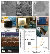
Graduate students Brian Goodfellow, Vahid Akhavan, and Matthew Panthani working under Prof. Brian Korgel at the University of Texas have developed a synthesis for CIGS nanocrystal “inks” that can be deposited from solution by a variety of techniques including drop-casting, dip-coating, spin-coating, spray-casting, and inkjet printing. These nanocrystal “inks” have been used to make functional photovoltaic devices with efficiencies greater than 3%. Conventional fabrication of CIGS solar cells is too expensive for widespread use so our development of CIGS nanocrystal-based “inks” provides a promising pathway for reducing these manufacturing costs by enabling solution-based methods to be applied to this demonstrated photovoltaic material.
Graduate students Micah Glaz and Dave Ostrowski working under Prof. David Vanden Bout at The University of Texas at Austin have developed a scanning optical microscopy-based approach at characterizing the performance of solar cells. This technique, which is called laser beam induced current (LBIC) microscopy, is applicable to a wide variety of solar cells and is especially interesting for solution-deposited materials with spatial heterogeneity.
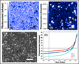
This technique has been used to characterize CIGS nanocrystal-based solar cells and the results revealed distinctive characteristics that led to a deeper understanding of the way in which the device functions. Solar cells were fabricated for this study by spray-depositing (also known as airbrushing) a light-absorbing layer of CIGS nanocrystals from an ink. LBIC microscopy maps of these devices revealed distinct features that correspond to high and low values of light-induced current when compared to the average local photocurrent in the device (see attached corresponding figure).
One of the most interesting characteristics of these LBIC maps are the channel-like regions of high photocurrent which correspond to very thin cracks that form when the deposited nanocrystal-based ink dries on the substrate. These cracks are actually not detrimental to the overall performance of the device and surprisingly were found to be the best performing areas of solar cell. We determined that this was due the reduced thickness of the light-absorbing CIGS nanocrystal layer in the cracks. One might think (as we did initially) that as you increase the amount of light-absorbing material, more light can be absorbed and converted into electricity. However, these experiments actually revealed the opposite to be true for these devices, thinner layers of the light absorber resulted in higher amounts of generated electricity. This point was subsequently confirmed by a separate experiment in which several devices were made with different thickness of the light-absorbing layer. In a solar cell, there is a built-in electric field that helps move electrical charges in the right direction. It was determined that in our devices, this electric field was only extending a couple of hundred nanometers into our light-absorbing layer and only the light absorbed in this thin layer was being converted to electricity. Thus, increasing the thickness of the absorber layer beyond this point only served to reduce the overall performance.
This synergetic collaboration has been proven to provide an effective feedback loop in the development of a novel solar cell technology and could perhaps be very beneficial for the field of solar energy as a whole. Further experiments are currently underway to take advantage of this by 1) characterizing nanocrystal-based light-absorbing layers that have been deposited by a variety of deposition techniques including drop-casting, dip-coating, spin-coating, spray-casting, and inkjet printing and 2) evaluating strategies to overcome thickness-related limitations in nanocrystal-based solar cells.
Address Goals
The objectives of this work have helped to accomplish several of the NSF’s strategic goals. First, a fundamental scientific understanding of specific properties of nanocrystal-based solar cells has been discovered through this collaborative effort. By setting up and demonstrating an effective feedback loop for the development of emerging solar cell technologies, this work can be further applied not only to the systems studied here but also to other solar cell materials, architectures, and processing techniques. Secondly, the building of an instrumental setup in order to study these devices has enhanced the scientific research infrastructure. This was accomplished because new experimental instruments were designed and built specifically to achieve the research goals of this work. Thirdly, this work was highly catalyzed by the interdisciplinary framework of the IGERT program and the nature of the specific IGERT theme to which these two students belong. The training of students to be pioneers and leaders in highly-collaboroative interdisciplinary research has been demonstrated. A similar outcome might not so easily follow from a program that does not emphasize the opportunity for achievement in interdisciplinary areas.
In summary, the real-life training of students in interdisciplinary collaborative research, the discovery and invention that have resulted in this work, and the development of research tools that promote scientific studies of solar technology are a direct result of the NSF-funded Integrative Graduate Education and Research Traineeship (IGERT) program in Atomic and Molecular Imaging of Interfaces and Defects at The University of Texas at Austin.