

Highlight Photo
Low temperature 3D wafers bonding for high speed and high density microchip applications
Low temperature 3D wafers bonding using Cu nanorods
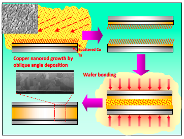
Figure 1. Schematic illustration of wafer bonding by Cu nanorod array at a temperature of <400°C. The inset in the upper left corner shows a SEM image of as-deposited Cu nanorods with ~10-30 nm diameter. The nanorods were deposited by the oblique angle deposition onto the wafers at room temperature using electron beam evaporation technique with pre-sputtered Ta and Cu films on the wafers. After the wafer bonding process the bonded region consists of homogeneous Cu grains.
Credits: Pei-I Wang
