

Highlight Photo
Patterned regrowth produces atomically thin, electrically active heterojunctions
Schematic illustration of patterned films
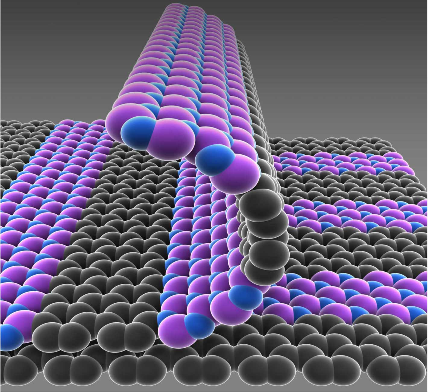
Single-atom-thick films with patterned regions of conducting graphene (gray) and insulating boron nitride (purple-blue) were grown with a new technique. The electronic properties of the stacked films confirm the utility of this approach.
Credits: Mark P. Levendorf
