
Highlight
Development of Processes Needed to Grow Single Crystal Silicon Nanowires from a Self-Assembly Patterned Array
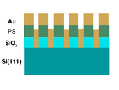
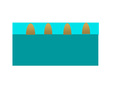
Fig 1 Schematic of the etch-transferred features with a gold film
Achievement/Results
This research was performed by Ben Spivey, an IGERT trainee, who is being advised by John Ekerdt who is an IGERT faculty member. We report the development of processes needed to grow single crystal silicon nanowires from a self-assembly patterned array. Self-assembly performed using the block copolymer PS-(b-MMA) is very sensitive to preprocessing steps, and we have identified process improvements required to ensure repeatable self-assembly. The self-assembled polymer produces a hexagonal array of 17 nm PMMA cylinders with a density of 6 × 1010 cm-2 that can be dissolved out with acetic acid leaving cylindrical voids in a continuous 36-nm polystyrene film. Using the polystyrene as an etch transfer mask, the 10-nm SiO2 film at the bottom of the cylinders is removed in a reactive ion etching step to reveal Si(111). Approximate 10 nm of gold is evaporated onto the polymer and into the cylindrical features (Figure 1). After depositing Au and performing liftoff (Figure 2), we have observed Au nanoparticle arrays having the same pattern and dimensions as the self-assembled polymer (Figure 3). Work this year will investigate Au nanoparticles as a catalyst for silicon nanowire growth after which we expect to submit results of the patterned growth for publication.
Address Goals
Discovery: The research seeks to determine: 1) the feasibility of precise positioning of nanowire seeds (the gold nanoparticles) of the requisite diameter to produce uniform and aligned nanowires using diblock copolymers as a templating mask; 2) the properties of nanowires seeded at the bottom of cylindrical vias and sitting atop the Si(111) surface that gives oriented nanowires; 3) the potential for altering the nanowire diameter and properties through the process that generates the size of the gold nanoparticles in a highly reproducible and controlled manner; and 4) the potential for dense arrays of nanowires to be incorporated into a massively parallel, and wired sensor system.
Learning: This program addresses learning in that it will combine the technical skills that include chemical processing, process control, nanoscale characterization of individual wires, and system integration into a sensor. These skills span numerous disciplines and progress toward an integrated sensor system will demonstrate how the breadth of knowledge is required to make advances. Students working on this program necessarily need to spend time working in the laboratories of crystal and film growers, polymer chemists, and spectroscopists, and they need to spend time working with systems engineers.
Infrastructure: If some of the patterning goals are realized this work will offer a new system for designing sensors.