
Highlight
Imaged defects in novel nanoparticle photovoltaic devices
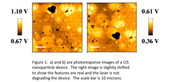
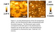
Figure 1: a) and b)Photoresponse images of a CIS nanoparticle device
Achievement/Results
National Science Foundation funded researchers at the University of Texas at Austin have imaged defects in novel nanoparticle photovoltaic devices. Two graduate trainees in the Integrative Graduate Education and Research Traineeship Program in Atomic and Molecular Imaging of Interfaces and Defects have started a collaborative research project to unravel the fundamental processes limiting the efficiency of Copper Indium Selenide (CIS) nanoparticle solar cells. Micah Glaz, a chemistry graduate student working with Prof. David Vanden Bout and Brian Goodfellow, a chemical engineering graduate student working with Prof. Brian Korgel combined the expertise of their respective research groups to achieve this success. The Korgel lab is working to develop new nanoparticle materials that can be used to manufacture efficient low cost photovoltaics. Mr. Glaz and co-workers examined devices that have been fabricated by Mr. Goodfellow and his research group. The devices have essentially four layers: a metal electrode, an active CIS layer, a buffer layer of CdS nanoparticles, and a transparent metal oxide electrode.
The question to be addressed was do defects in the device limit its efficiency. This was answered in a straightforward experiment in which the solar cell was illuminated with a highly focused laser spot to examine if shining light on different regions within the device led to differences in the current generated. Figure 1 shows that there were dramatic differences from different regions within the sample. The image shows the current detected by scanning the laser spot across the device. (The scale is a voltage scale because the small currents generated from microscopic regions in the device require amplification in which they are converted to voltage signals). Clearly some regions have low efficiencies (dark) and some a significantly higher (bright). The two images are of the same region that has a slight spatial shift to demonstrate both response is reproducible and that the laser is not altering the material.
While the imaging shows regions of different response what is fundamentally import is the reason behind the efficiency difference. This was determined by simultaneously imaging the luminescence from the device along with the induced photocurrent. Photovoltaic materials should not be luminescent because in an ideal case all of the light that is absorbed would be converted to electrical energy. Figure 2 shows simultaneously collected images of the photocurrent and the luminescence. There is an obvious correlation between the regions of low efficiency and the regions in which there is luminescence. Because the CIS nanoparticles themselves are not inherently luminescent, the emission must have a different source. The device has a thin layer of CdS nanoparticles between the active CIS material and the metal oxide electrode. The CdS material can be extremely emissive. The images demonstrate the defects in the fabrication lead to regions in which the CdS layer is much thicker. This not only leads to some of the absorbed light energy being re-emitted, but it also prevents charge from arriving at the metal oxide electrode. In addition to the regions of low photocurrent, there are regions that are substantially better than others.
The goal now is to fabricate devices in which all of the response is as large as these small extremely efficient regions. By combining the science and engineering of these two research groups we have been able to quickly assess how defects are limiting the efficiency of these devices as well as develop strategies to greatly improve their efficiency.
Address Goals
One of the challenges to discovery and advancement in modern science and engineering is the need for interdisciplinary research. The project initiated by trainees Micah Glaz and Brian Goodfellow clearly demonstrates how partnerships between scientists and engineers can lead to richer discoveries than either isolated discipline. This is a direct result of the IGERT program in Atomic and Molecular Imaging of Interfaces and Defects at the University of Texas at Austin. This program brings students into contact with each other through interdisciplinary classes and regular meeting and seminars. It actively encourages interdisciplinary collaboration through the programs capstone laboratory course and its newly implemented research proposal program. Mr. Glaz and Mr. Goodfellow were the first researchers selected for funding in this initial proposal competition. In their work together both have learned from each other as they work towards a common goal. This has allowed them not only push forward the fundamental understanding of these nanoparticle photovoltaic devices, but has served as a new model for graduate education.