

Highlight
Patterned regrowth produces atomically thin, electrically active heterojunctions
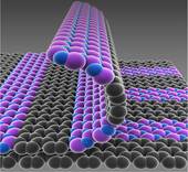
Schematic illustration of patterned films
Achievement/Results
Working with a team of interdisciplinary scientists at Cornell University, IGERT Fellow Mark Levendorf has produced precisely patterned, single-atom-thick sheets to enable the ultimate in microfabrication miniaturization. Microelectronic devices, such as computers, are based on integrated circuits: thin films with precisely patterned insulating, semiconducting, and conducting regions stacked one upon the other to form three-dimensional circuits. Miniaturizing these devices to the ultimate limit — a stack of single-atom-thick sheets — is a formidable challenge that is conceptually similar to knitting atomically thin, precisely patterned scarves that have no holes, breaks, or gaps and then aligning the scarves perfectly in a wrinkle-free stack.
Researchers at Cornell University have developed a new technique, ”patterned regrowth,” that enables the first step: creating precisely patterned, single-atom-thick films. Instead of knitting the patterned scarf from one end to the other, they grow a single-atom-thick sheet of the first material, maybe the semiconductor, then cut it to the desired shape using standard nanofabrication techniques. The next step is key: they grow the second material, maybe an insulator, out from the cut edges of the first, creating an electrically and mechanically sound “heterojunction.” The second material is then cut in the desired shape and the process repeated until the patterned sheet is complete. The development of this simple but robust technique is an important step towards the production of atomically-thin integrated circuits. Figure caption: Schematic illustration of experiment: Single-atom-thick films with patterned regions of conducting graphene (gray) and insulating boron nitride (purple-blue) were grown with a new technique. The electronic properties of the stacked films confirm the utility of this approach.
*Levendorf, M. P., Kim, C.-J., Brown, L., Huang, P. Y., Havener, R. W., Muller, D. A., & Park, J. (2012). Graphene and Boron Nitride Lateral Heterostructures for Atomically Thin Circuitry. Nature, 488, 627–632.
Address Goals
Discovery: The development of new approaches for the growth of single-atom-thick films with patterned heterostructures of conducting and semiconducting material is an important step towards the production of atomically-thin integrated circuits. Learning: This highly interdisciplinary and integrative research project required the sustained contributions of scientists with a wide range of talents and expertise. This interdisciplinary milieu provided an ideal training ground for next-generation scientists and engineers educated in cutting-edge nanoscience.
